Diamond heat dissipation has become the core material solution to break the "thermal barrier" bottleneck of high-power devices such as AI, supercomputing and 5G. With its extreme thermal conductivity, electrical insulation and high stability, it is moving from laboratory research to large-scale commercial application, and 2026 is regarded as the first year of its commercialization. This paper conducts a detailed analysis from the perspectives of working principle, core properties, advantages and disadvantages, market space, commercialization progress and future development potential.
I. Heat Dissipation Principle
The core advantage of diamond heat dissipation stems from its atomically compact crystal structure and unique phonon heat conduction mechanism:
- Crystal Structure: Diamond forms a regular tetrahedral spatial network structure through sp³ hybridization of carbon atoms, featuring extremely short atomic bond length and ultra-high bond energy, allowing lattice vibration (phonon) propagation with almost no obstruction.
- Heat Conduction Mechanism: Heat transfer relies mainly on phonon conduction while electronic heat conduction is negligible. Phonons possess an extremely long mean free path and fast thermal diffusion speed, enabling instantaneous and uniform transfer of heat from local hotspots to the entire heat sink.
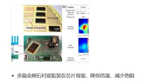
- Near-Junction Heat Dissipation Advantage: Diamond features excellent electrical insulation and can be directly attached to bare chip dies without additional insulating layers. It eliminates interfacial thermal resistance and builds an efficient thermal path of Chip – Diamond – Heat Dissipation System.
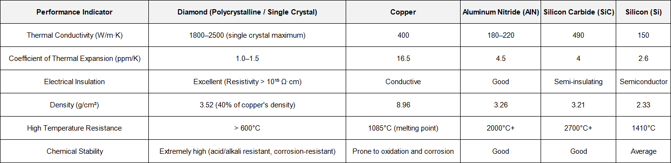
II. Core Properties (Comparison with Traditional Materials)
- Extreme Thermal Conductivity: Its thermal conductivity is 5–6 times that of copper, 4–5 times that of SiC, and 13 times that of silicon. It is the only material option for scenarios requiring thermal conductivity above 500 W/m·K.
- Low Thermal Expansion: Its coefficient of thermal expansion is highly matched with semiconductors such as Si, GaN and SiC, reducing thermal cycling stress and improving device reliability.
- Electrical Insulation & High Stability: It can be directly used as heat dissipation substrates and heat sinks without insulating layers; it also features high temperature resistance and corrosion resistance, suitable for extreme operating environments.
- Lightweight Advantage: Its density is only 40% of copper, with a thermal conductivity-to-density ratio far exceeding metal materials, facilitating equipment weight reduction
III. Analysis of Advantages and Disadvantages
Core Advantages
- Ceiling-level Heat Dissipation Efficiency: Rapidly dissipates chip hotspot heat, reduces junction temperature by 20–70℃, suppresses frequency throttling, and releases 10%–40% of chip performance.
- System-level Benefits: Cuts data center heat dissipation energy consumption by 40%, raises single cabinet power density to over 900kW, and significantly improves computing density and energy efficiency ratio.
- Enhanced Reliability: Matched low thermal expansion and high structural stability extend device service life and reduce failure rates.
- Multifunctional Integration: It can serve as structural support parts simultaneously, simplifying heat dissipation system design and reducing overall volume and weight.
Main Disadvantages
- High Cost: The growth process and equipment for electronic-grade single-crystal and large-size polycrystalline diamond (such as MPCVD) are highly complex, with unit prices over a hundred times higher than copper.
- Difficult Processing: With a Mohs hardness of 10, diamond is extremely hard to cut, polish and drill, resulting in low yield and further increased costs.
- Interface and Integration Challenges: Lattice mismatch and thermal expansion difference with GaN, Si and other materials make direct epitaxy difficult. Bonding and composite processes are required, inevitably increasing interfacial thermal resistance.
- Size Limitation: Mass production of large-size (≥ 4-inch) low-warpage diamond wafers is still in the breakthrough stage, unable to meet the demand for ultra-large chips.
IV. Market Space (2026–2030)
1. Market Scale
- 2026: The global market size is about 1.2–1.5 billion US dollars, with China accounting for over 50%.
- 2030: Expected to reach 10–15 billion US dollars with a CAGR exceeding 60%, becoming the fastest-growing segmented market in the thermal management industry.
2. Core Application Fields
AI Computing / Supercomputing (Largest Driving Force)
High-end GPU/AI chips (700W–2000W power consumption) and supercomputing centers adopt diamond-copper composite heat sinks and diamond thin-film substrates.
Case: NVIDIA H200 servers and national supercomputing internet nodes have achieved commercial application, with single cabinet power density increased by 3 times.
5G/6G Communication
Used for GaN RF power devices and base station power amplifiers. Diamond heat dissipation boosts the power density of GaN devices by over 40% and reduces junction temperature by 36%.
New Energy Vehicles
Applied to SiC power modules, vehicle LiDAR and autonomous driving domain controllers, providing high-temperature resistant and highly reliable heat dissipation solutions.
Military & Aerospace
Serving radar and satellite payloads with high stability and lightweight heat dissipation under extreme environments.
Consumer Electronics (Medium and Long Term)
High-end smartphones, VR/AR devices adopt ultra-thin diamond thin films for chip near-junction heat dissipation, solving overheating problems of high-refresh screens and high-computing chips.
3. Advantages of China’s Market
- Raw Material Dominance: China’s synthetic diamond output accounts for over 95% of the global total, realizing independent supply of powder and single crystal materials.
- Technological Breakthroughs: The localization rate of MPCVD equipment exceeds 60%; 4-inch diamond wafers and diamond-copper composite materials have achieved mass production.
- Cost Advantage: The cost of domestic products is only 1/3 of international counterparts, with outstanding cost performance.
V. Commercialization Process (2026: The First Year of Commercialization)
1. Main Technical Routes and Maturity
Diamond-Metal Composite Material (Fastest Industrialization)
Route: Compound diamond particles with copper/aluminum to balance high thermal conductivity, machinability and controllable cost.
Breakthrough: In April 2026, the diamond-copper composite material developed by Ningbo Institute of Materials Technology and Engineering, CAS achieved a thermal conductivity exceeding 1000 W/m·K, realizing the world’s first large-scale cluster deployment on the national supercomputing internet.
Application: Server heat sinks, liquid cooling modules and power module heat dissipation.
Self-Supporting Diamond Wafers / Thin Films (High-End Route)
Route: Grow large-size low-warpage diamond sheets via MPCVD, directly used as chip substrates and heat sinks.
Breakthrough: China Electronics Technology Group realized mass production of low-cost 4-inch diamond wafers; Ningbo Institute of Materials prepared 4-inch ultra-low warpage (<10μm) diamond thin films.
Application: GaN-on-Diamond devices and near-junction heat dissipation for high-end AI chips.
Diamond Thin-Film Deposition / Bonding (Integrated Route)
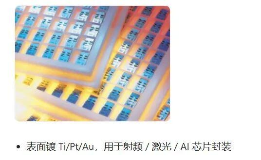
Route: Deposit ultra-thin diamond films on the surface of chips or heat sinks, or integrate diamond with chips through Surface Activation Bonding (SAB).
Application: Heat dissipation for RF and optoelectronic devices.
2. Commercialization Milestones (2025–2026)
- 2025: NVIDIA and Huawei completed verification of diamond heat dissipation solutions and entered supply chain certification.
- Q1 2026: The world’s first micro-nano diamond production line was put into operation; Huifeng Diamond’s annual 2 billion carat diamond powder project was approved.
- Q2 2026: Diamond-copper composite materials were commercially deployed on a large scale in supercomputing centers; 4-inch diamond wafers started small-batch supply.
- Q2 2026: Huanghe Whirlwind, Lizard Diamond and other enterprises entered the supply chain of NVIDIA and Huawei with small-batch deliveries.
3. Stage Characteristics
- Completed breakthrough from 0 to 1: Core technological breakthroughs passed verification in high-end scenarios and began large-scale implementation.
- Rapid cost decline: Equipment localization and process optimization drive annual cost reduction of over 30%, with cost performance gradually emerging.
- Accelerated layout by industry giants: NVIDIA, Intel, TSMC, Huawei and other enterprises deploy diamond heat dissipation, promoting industrial standardization.
金属化 CVD 金刚石热沉(可直接焊芯片)
VI. Industry Status
The inflection point of mass production has arrived, driven by explosive market demand and domestic substitution.
1. Core Driving Forces: AI Thermal Bottleneck + Policy Support
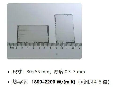
- Surge in AI chip power consumption: The power consumption of NVIDIA Rubin architecture GPU reaches 2300W, while traditional copper (400W/m·K) and aluminum (200W/m·K) heat dissipation have reached their limits. With a thermal conductivity of 1800–2200 W/m·K (4–5 times that of copper), diamond can lower GPU junction temperature by 50–70℃ and boost computing power release by 3 times.
- Downstream demand boom: AI servers, supercomputers, 5G/6G base stations, radar T/R components, new energy vehicle electronic control, satellite aerospace and other fields see concentrated demand growth; 2026 is defined as the first year of diamond heat dissipation mass production.
- Policy and capital support: Military mass production and semiconductor independent controllability policies under China’s 15th Five-Year Plan boost industrial development; institutions forecast the global market will grow from 50 million US dollars in 2025 to 15.2 billion US dollars in 2030, with a CAGR of 214%.
2. Technical Routes: CVD as the Mainstream, Three Generations of Domestic Evolution
- Mainstream Technology: MPCVD (Microwave Plasma Chemical Vapor Deposition) dominates 90% of the market for preparing high-thermal-conductivity diamond heat sink sheets; HPHT (High Pressure High Temperature) is mainly used for diamond/copper composite substrates with low cost and high strength.
- Three-Generation Technological Upgrade:1st Generation (2018–2022): Plane carrier sheet, thermal conductivity 1200–1500 W/m·K, applied in military and radio frequency fields.2nd Generation (2023–2025): Micro-channel heat sink, thermal conductivity 1800–2000 W/m·K, small-batch application in AI servers.3rd Generation (2026– ): Integrated packaging shell, thermal conductivity 2000–2200 W/m·K, compatible with 2000W+ GPU and ready for large-scale mass production.
- Domestic Gap: Basic materials and high-end equipment are slightly inferior to international leaders such as Akash (USA) and Element Six (UK), but domestic enterprises have obvious advantages in application innovation, cost control and service response, keeping pace or even leading in some technical indicators.
3. Production Capacity & Price: Rapid Expansion and Sustained Cost Reduction
- Capacity Expansion: China’s planned annual production capacity will reach 500,000–800,000 pieces (8-inch equivalent) in 2026, a 5–10 times increase compared with 2025; Huanghe Whirlwind, Lizard Diamond and Sinomach Precision form the first echelon.
- Price Trend: The price of 8-inch heat sink sheets dropped from 12,000 RMB per piece in 2023 to 3,000–4,000 RMB in 2026, with an annual decline of 40–50%, approaching the critical point of large-scale commercialization.
- Yield Improvement: The yield of leading enterprises reached 85–90% in Q2 2026, a significant improvement from 60%–70% in 2024, supporting continuous cost reduction.
4. Competitive Pattern: Six Leading Enterprises Dominate, Domestic Substitution Accelerates
- First Echelon (Technology + Capacity + Customer Barriers): Huanghe Whirlwind, Lizard Diamond, Sinomach Precision.
- Second Echelon (Technical Reserve + Small-Batch Supply): Sifangda, Wold, Norinco Red Arrow.
- International Giants: Akash Systems (USA, commercially applied in NVIDIA H200 / AMD MI350X servers), Element Six (UK), Sumitomo Electric (Japan). Domestic enterprises have entered the supply chain of NVIDIA and Huawei since 2026, breaking the international monopoly.
VII. Future Development Potential (2027–2035)
1. Technological Evolution Directions
- Size & Quality Upgrade: Realize mass production of 6-inch diamond wafers in 2027, and break through 8-inch wafers in 2030 to meet the demand of advanced process chips.
- Cost Revolution: Improved MPCVD efficiency and large-scale production will reduce the cost of diamond heat dissipation materials by over 70% in 2030 compared with 2026, entering the price range of less than 100 US dollars per piece.
- Integrated Innovation: Mature heterogeneous integration technology of diamond with GaN and SiC realizes integrated device-heat dissipation design; micro-channel diamond heat sinks and 3D stacked heat dissipation solutions achieve commercial application.
- Application Expansion: Penetrate from high-end computing and communication to mass markets such as new energy vehicles and consumer electronics.
2. Industrial Pattern Outlook
- China’s Leading Position: The domestic localization rate will rise to over 70% by 2030, making China the global center of diamond heat dissipation technology and production capacity.
- Material Substitution: In scenarios requiring thermal conductivity above 500 W/m·K, diamond will gradually replace copper, AlN and SiC to become the mainstream heat dissipation material.
- Improved Industrial Ecosystem: Form a complete industrial chain of Diamond Raw Material → MPCVD Equipment → Wafers / Composite Materials → Heat Dissipation Devices → Terminal Application.
3. Ultimate Value
Diamond heat dissipation is not merely a cooling material, but an infrastructure for the computing revolution.
- Support single-chip power consumption breakthrough from 2000W to over 5000W, unlocking next-generation AI and quantum computing power.
- Promote the evolution of data centers from air cooling to liquid cooling + diamond composite heat dissipation, reducing PUE below 1.1 and realizing green computing.
- Provide independently controllable thermal management solutions for strategic industries such as 6G communication, Starlink and new energy vehicles.

The Mitac G8825Z5 8-card server features each MI350X equipped with a diamond heat sink. Released in March 2026, it has an order value of approximately $300 million, with a 15%–22% increase in computing power under high temperatures.
Summary
With incomparable thermal properties, diamond heat dissipation has become the core solution to break the thermal barrier of high-power chips. 2026 marks its first year of commercialization, with initial large-scale application in AI, supercomputing and communication fields. In the next five years, along with cost reduction and technological maturity, it will rapidly expand into more high-end manufacturing fields, reshape the global thermal management industrial pattern, and become the cornerstone of heat dissipation in the computing era.

 Scan to contact us
 Scan to view the mobile version