
TEL:13526590898
 Scan to contact us
 Scan to view the mobile version

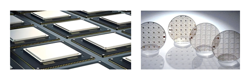
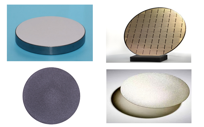
Bonding Routes: Single-crystal SiC bonded to polycrystalline SiC, semiconductor-grade single-crystal Si bonded to diamond, single-crystal SiC bonded to diamond, GaN bonded to diamond, Si₃N₄ bonded to diamond.
Deposition Routes: Semiconductor-grade diamond-on-substrate materials including diamond on single-crystal silicon, diamond on single-crystal SiC, diamond on GaN, diamond on Si₃N₄, diamond on polycrystalline SiC, and diamond on AlN.
Application Scenarios:
Bonding: Backside heat spreaders, high-power, high-flux, high-end RF / automotive-grade power devices.
Deposition: Frontside thin films, integrated coatings, medium-to-low power, specialty sensors / small packages.
Advantages
Bonding — Common Strengths
Low process temperature, no damage to semiconductor epitaxial films
High-thermal-conductivity single/polycrystalline diamond substrates enable higher cooling ceilings
Controllable interface with optimized low interfacial thermal resistance
Independent processing of both substrates with pre-screening of defects, improving final yield
Deposition — Common Strengths
Monolithic growth — no bonding voids or delamination risks
Ideal for front-side diamond thin-film fabrication on devices
Suited for large-scale continuous coating, with cost potential for mid/low-power applications