
TEL:13526590898
 Scan to contact us
 Scan to view the mobile version

I. Diamond Laser Pump Sources
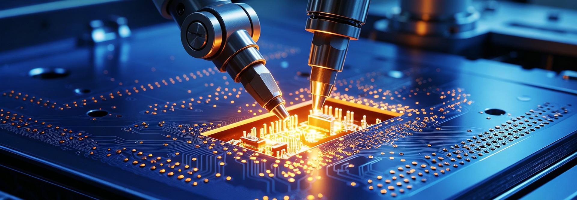
The core concept is replacing traditional copper, MoCu, or CuW heat sinks with CVD single-crystal diamond as the packaging heat spreader for LD chips, breaking through power density and lifetime bottlenecks via thermal management.
1. Operating Principle & Heat Flow Path
During LD operation, Joule heat from the active region accounts for ~30–50% of input electrical power. Heat is extracted via: LD junction → solder layer → diamond heat spreader → secondary water-cooling / micro-channel cooler.
With ultra-high room-temperature thermal conductivity of 1200–2200 W/m·K, diamond rapidly spreads and extracts junction heat, keeping junction temperature variation within 5°C — effectively suppressing thermally induced wavelength drift (~0.3 nm/°C for LDs), beam distortion, and optical power degradation, ultimately boosting maximum output power, electro-optical efficiency, and long-term reliability.
2. Key Advantages (Quantified Comparison)
vs. traditional oxygen-free copper heat spreaders, diamond-based pump sources deliver three core improvements:
Significantly Lower Thermal Resistance: 40–60% reduction for same footprint. For a 10×10×1 mm spec: single-crystal diamond ~0.15 °C/W vs. OFHC copper ~0.38 °C/W. Allows 30%+ higher LD operating current density, with single-bar output power density nearly doubling.
Better CTE Matching: Diamond CTE ~1.5×10⁻⁶/°C, far closer to GaAs-based LD chips (~6.5×10⁻⁶/°C) than copper (17×10⁻⁶/°C). Packaging thermal stress reduced by 70%+, preventing chip cracking and solder fatigue under thermal cycling.
High Damage Threshold & Insulation: Diamond is intrinsically insulating, enabling direct electrical isolation between chip and base. Optical damage threshold >10 GW/cm² (nanosecond pulse), suitable for compact optical designs such as high-power end-pumping and spatial combining.
II. Diamond Laser Galvanometer Scanner Mirrors
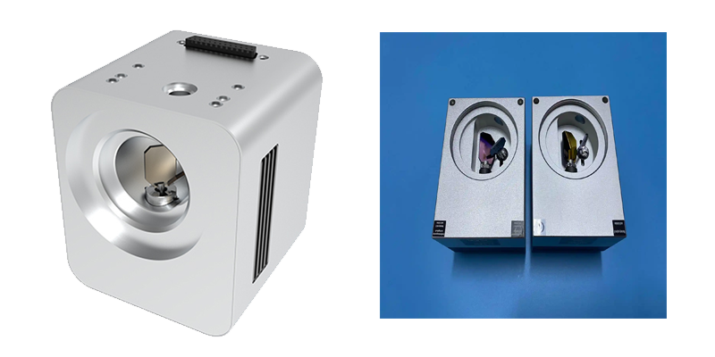
In laser galvanometer systems, diamond serves as the substrate material for the scanning mirror. For kW-class and above (especially 10kW+ CW/ultrafast laser) scanning applications, it fundamentally solves the thermal deformation and thermal lensing effects that plague conventional copper, silicon, or SiC mirrors under high-power irradiation — ensuring scanning accuracy, beam quality, and long-term reliability. This represents a premium upgrade for high-power laser galvanometers.
The galvanometer mirror directly carries the laser beam. Under high-power irradiation, the mirror absorbs a small fraction of laser energy, causing temperature rise and surface thermal expansion (thermal lensing), which directly leads to beam drift, focus degradation, and positioning errors. In severe cases, coating damage or even mirror fracture may occur.
Diamond, with its ultra-high thermal conductivity and extremely low CTE, rapidly spreads and extracts absorbed heat from the mirror surface while limiting thermal deformation to the nanometer scale:
Typical Application Scenarios
10kW+ Galvanometer Laser Welding: Power battery cell welding, automotive structural parts, new-energy motor stator welding — paired with high-power diamond heat-sinked pump sources, solving beam drift and weld consistency issues in long-duration continuous processing.
High-Power Ultrafast Laser Galvanometer Processing: PCD/PCBN super-hard tool laser etching and dressing, semiconductor wafer stealth dicing — diamond mirrors withstand high-peak-power pulses without coating damage or thermal accumulation deformation.
Aerospace Galvanometer Cladding / Surface Treatment: High-speed scanning cladding and surface strengthening of large structural components — stable long-term operation at high power, reducing maintenance downtime.
R&D & Specialized Laser Systems: High-energy laser scanning, terahertz beam scanning, high-power laser experimental setups, and other extreme-condition applications.