TEL:13526590898
 Scan to contact us
 Scan to view the mobile version
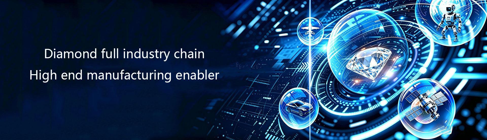
2026 is hailed by the industry as the inaugural year for the industrialization of diamond heat dissipation. NVIDIA invested USD 2 billion in strategic investment in Coherent to lock in diamond production capacity; AMD simultaneously launched diamond-cooled servers; China’s first 8-inch diamond heat sink wafer production line was put into operation in Xuchang. Behind these seemingly scattered events lies one undeniable fact: diamond is evolving from “the hardest material” into “the most sought-after thermal management material”.
This emerging trend did not arrive unexpectedly; it represents a critical breakout after decades of technological accumulation. As silicon-based chips approach physical limits and the power density of AI computing power surpasses the ceiling of air cooling, humanity has begun to re-examine diamond — the material with the highest thermal conductivity on Earth.
To understand why diamond has become the protagonist in the heat dissipation track, one must first grasp its inherent material genes.
Diamond is an sp³ hybrid crystal of carbon, where carbon atoms form a three-dimensional network structure through extremely strong covalent bonds. This dense crystal structure endows it with two unparalleled physical properties: unrivaled hardness and supreme thermal conductivity.
At 23°C, diamond achieves a thermal conductivity as high as 2200 W/(m·K), 5 times that of copper, 13 times that of silicon, and 4.5 times that of silicon carbide. What does this mean?
Heat conduction in materials can be analogized to water flowing through pipelines. Ordinary materials are like cracked earthen pipes with high thermal resistance and massive energy loss; diamond, by contrast, acts as an absolutely smooth superconducting channel, allowing heat to dissipate with almost no loss.
More importantly, diamond features a breakdown electric field of 10 MV/cm — 33 times that of silicon and 2.5 times that of silicon carbide. It can withstand far higher voltage without breakdown, operating stably under extreme conditions such as high voltage, high temperature and intense radiation.
These unique properties secure diamond a special position in the generational evolution of semiconductor materials. The industry generally classifies semiconductors into four generations:
Given diamond’s exceptional heat dissipation performance, why has it not been widely applied before now? The answer lies in three major bottlenecks: cost, wafer size and mass production capacity.
In the past, diamond heat sink wafers were mainly manufactured by the High Pressure High Temperature (HPHT) method, limited in size and prohibitively costly, only applied in small-batch high-value scenarios such as national defense and military industries. Although the Chemical Vapor Deposition (CVD) method can theoretically produce large-size diamond films, low process maturity and poor yield long restricted industrialization.
In 2026, three landmark signals emerged simultaneously, marking the arrival of the inflection point.
In March 2026, computing giant NVIDIA announced a USD 2 billion strategic investment in thermal management enterprise Coherent to secure the production capacity of diamond-SiC liquid cooling plates. In the same period, AMD launched diamond-cooled servers based on the MI350X platform. Server vendor Akash Systems delivered the world’s first batch of diamond-cooled H200 servers to Indian clients and secured a USD 300 million order.
Most notably, at GTC 2026, NVIDIA officially announced that next-generation Rubin and Feynman architecture GPUs will fully adopt the standard diamond + liquid cooling thermal management solution.
The collective endorsement by top global chip vendors signifies that diamond heat dissipation has upgraded from an optional alternative to a must-have standard solution.
In March 2026, China’s first 8-inch diamond heat sink wafer production line was commissioned in Xuchang, Henan. Adopting MPCVD technology, it is designed with an annual capacity of 20,000 wafers. Its products have passed verification by Huawei, SMIC and BYD, with pending orders worth approximately RMB 150 million.
In the same month, the LPPHT micro-nano diamond production line of Zhongke Fenyan started operation, achieving a yield rate of 92.7% — 30 percentage points higher than the industry average. The entire production process is fully domestically controllable, with costs 27% lower than similar foreign products.
This milestone marks the official transition of diamond thermal management materials from laboratory R&D to large-scale mass production.
Measured data shows that integrating diamond heat dissipation can lower GPU junction temperature by 10–15°C and improve energy efficiency by 15–22%. Under a chip hotspot power density of approximately 2 W/mm², adopting a diamond heat sink substrate reduces the maximum chip junction temperature by up to 24.1°C and cuts packaging thermal resistance by 28.5%.
What do these figures mean? For AI data centers pursuing extreme computing density, every 1°C reduction in chip temperature enables stable operation at higher frequencies and greater computing output. The performance gains brought by diamond heat dissipation are far more than merely “cooler chips”.
If diamond’s value lay only in heat dissipation, it would remain merely a high-performance thermal management material. Yet diamond’s ambition stretches far further — its ultimate goal in the semiconductor industry is to become the ultimate semiconductor material.
As new energy vehicles upgrade to 800V high-voltage platforms, 5G base stations evolve toward millimeter wave communication, and radar systems advance toward terahertz technology, traditional silicon devices face prominent overheating and thermal runaway issues under high voltage and large current.
Diamond’s ultra-high thermal conductivity and breakdown field strength make it the ideal solution to this pain point. Taking the GaN-on-Diamond structure as an example: directly bonding a diamond substrate beneath the GaN epitaxial layer to replace traditional SiC or silicon substrates reduces junction temperature by 50% and boosts power density by 3 times.
At present, Element Six (under the De Beers Group), Raytheon and Infineon lead this field in global research. The team led by Professor Hongxing Wang at Xi’an Jiaotong University has realized batch production of 2-inch heteroepitaxial single-crystal diamond, reaching world-leading standards.
Nevertheless, the practical application of diamond semiconductors hinges on breaking a core bottleneck: n-type doping.
The core of semiconductor devices lies in the PN junction, which requires both n-type doping (providing electrons) and p-type doping (providing holes). P-type doping of diamond is relatively mature, while n-type doping remains challenging: the phosphorus atom radius is 1.4 times that of carbon, easily causing lattice defects after doping; meanwhile, phosphorus has an ionization energy as high as 0.6 eV in diamond, leading to extremely low ionization efficiency at room temperature.
In February 2026, the U.S. Argonne National Laboratory made new progress: its research team constructed heterostructures by stacking 2D materials such as MoS₂ on diamond, bypassing traditional doping limitations and achieving a breakthrough improvement in electrical performance. This offers a new pathway for the practicalization of diamond electronic devices.
While diamond’s application in power electronics still requires time to mature, it has shown immediate commercial potential in quantum computing.
The nitrogen-vacancy (NV) center in diamond is a unique quantum defect structure: a nitrogen atom replaces a carbon atom in the diamond lattice, with an adjacent atomic vacancy. This structure maintains highly stable electron spin states at room temperature and supports initialization, manipulation and readout via optical methods.
This is revolutionary. Traditional superconducting and ion-trap quantum qubits require near absolute zero temperatures (millikelvin level), with extremely complex and costly refrigeration systems. In contrast, quantum qubits based on diamond NV centers can operate stably at room temperature, greatly reducing system complexity and technical barriers.
In 2025, quantum tech firm Quantum Brilliance delivered room-temperature quantum computing systems to Germany’s Fraunhofer IAF and the U.S. Oak Ridge National Laboratory. The company also collaborated with IMEC, Europe’s leading semiconductor research center, to explore integrating diamond into 12-inch CMOS-compatible process lines.
Equally exciting is the breakthrough in quantum gate fidelity. Researchers at Delft University of Technology achieved world-record fidelity of 99.9991% for single-qubit gates and 99.935% for two-qubit gates using diamond NV centers, laying a solid foundation for quantum error correction and practical quantum algorithms.
Reviewing technological progress since 2026, several cutting-edge directions stand out:
Conventional diamond features a cubic crystal structure (cubic diamond), while nature possesses an even harder hexagonal diamond (also known as Lonsdaleite), rarely found only in meteorite impact craters.
In March 2026, the research team led by Professor Chongxin Shan at Zhengzhou University achieved millimeter-scale pure-phase hexagonal diamond under conditions of 20 GPa and 1300°C after five years of research, obtaining atomic-level structural evidence. The achievement was published in Nature, proving hexagonal diamond is not a hypothetical material but a stably manufacturable solid substance.
Earlier, the team led by Professors Bingbing Liu and Mingguang Yao at Jilin University published findings in Nature Materials, synthesizing high-quality bulk hexagonal diamond for the first time. It achieves a hardness of 155 GPa — 40% higher than cubic diamond — with thermal stability exceeding 1100°C.
In 2025, a study published in Nature Communications achieved a major breakthrough: adopting high-frequency pulsed local non-equilibrium growth technology, MPCVD was used to fabricate binder-free ultra-hard diamond wafers with a diameter of 5 inches, thickness of 3 mm, and Vickers hardness of approximately 208 GPa.
For reference, natural diamond has a Vickers hardness of around 110 GPa. This wafer nearly doubles the hardness of natural diamond, comparable to nano-twinned diamond, while breaking the previous size limit of conventional CVD production.
Diamond’s inherent brittleness has long restricted its application scenarios. The joint research team led by Professor Chongxin Shan at Zhengzhou University realized the large-scale preparation of flexible diamond films. The films can bend 360 degrees, combining ultra-high hardness, thermal conductivity and flexibility, suitable for chip heat dissipation, flexible electronics, biomedical and other fields.
Based on technological progress and industrial dynamics, the VestLab research team forecasts the commercialization roadmap for diamond semiconductors in three phases:
Q: Are lab-grown diamonds and industrial diamond the same material?
A: Fundamentally yes — both are pure diamond crystal. The difference lies in application positioning: lab-grown diamonds prioritize gem-grade indicators such as color and clarity for jewelry use; industrial diamond focuses on functional performance including thermal conductivity, hardness and purity. They also differ slightly in preparation processes and quality control standards.
Q: Is diamond heat dissipation too expensive for widespread use?
A: It is currently more costly than traditional cooling solutions, but costs are declining rapidly. Taking 2-inch diamond heat sink wafers as an example: the average price was about RMB 15,000 per piece in 2023, dropped to RMB 5,000 in 2025, and is expected to fall further to RMB 2,000 by 2027. With the commissioning of 8-inch production lines and rising yield rates, scale effects will accelerate cost reduction.
Q: How strong is China’s domestic diamond industry?
A: China dominates global industrial diamond production with over 90% of global capacity, yet still lags behind international leaders in high-end electronic-grade diamond. Domestic enterprises already have mass production capability for heat sink wafers and quantum-grade diamond, but large-size single-crystal diamond and high-purity diamond films still rely partially on imports or remain in the R&D stage. After China implemented new export control regulations for superhard materials in 2025, the process of domestic substitution has accelerated significantly.
Q: Will ordinary consumers be able to use products with diamond heat dissipation?
A: In the short term, diamond heat dissipation will be mainly deployed in high-value scenarios such as AI servers, data centers and 5G base stations. However, with falling costs and technological maturity, it is expected to penetrate high-end smartphones, new energy vehicles and other consumer electronics within 3–5 years. Some smartphone manufacturers have already tested diamond cooling solutions in flagship models.
As the classic slogan “A diamond is forever” still lingers in people’s minds, diamond has embarked on a new journey: from a gem symbolizing eternal love to a core material underpinning AI computing power. It is arguably one of the most romantic stories in materials science: a crystal composed of identical carbon atoms carries humanity’s longing for eternity, while quietly reshaping the underlying infrastructure of the next industrial revolution.