TEL:13526590898
 Scan to contact us
 Scan to view the mobile version

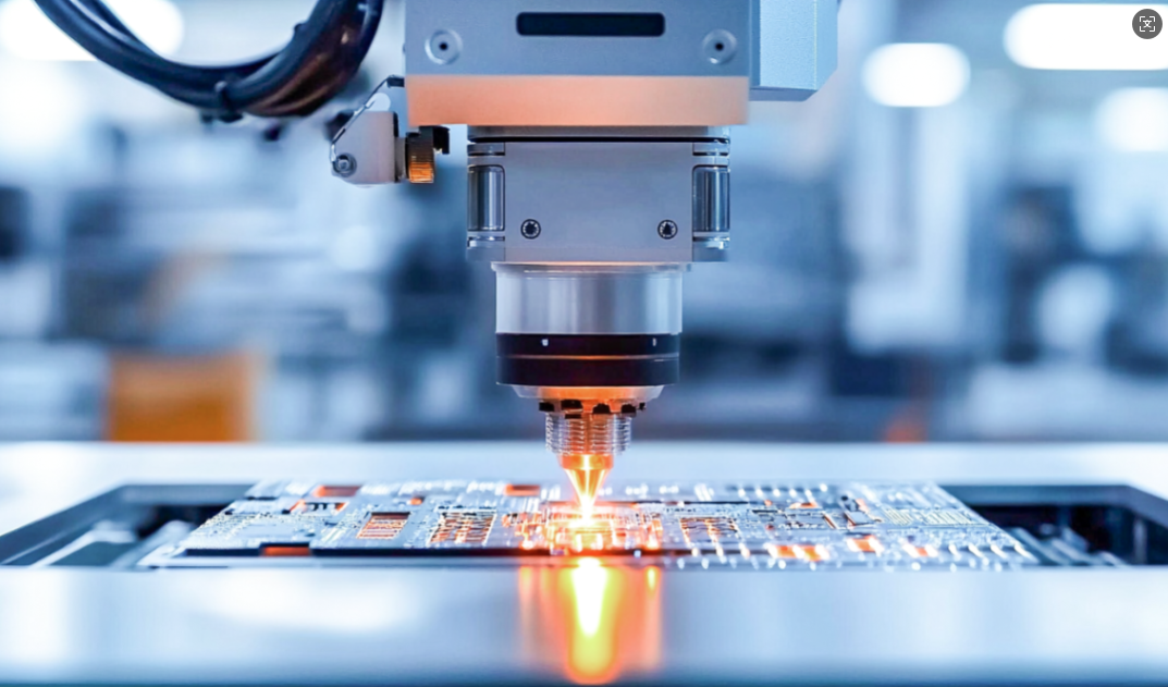
At the beginning of 2026, the thermal management technology in the AI computing power field ushered in a milestone breakthrough. At the beginning of the year, NVIDIA officially released the Rubin architecture, the next-generation AI computing platform, and announced the introduction of CVD diamond chips into its high-end chip products. Just two months later, the industry witnessed another significant progress in commercialization. Akash Systems announced its partnership with NxtGen AI Pvt Ltd to deliver the world's first NVIDIA H200 GPU servers equipped with Diamond Cooling® technology, which are powered by AMD Instinct™ MI350X GPUs and manufactured by MiTAC Computing (3706.TW).

This action is not a conventional iteration of traditional cooling solutions, but a landmark breakthrough extending from chip architecture design to the underlying material system as AI computing power develops to the ultra-high power density stage. When the power consumption of a single AI chip exceeds 1000W and the core's extreme hot spot heat flux density reaches the order of magnitude of approximately 1000W/cm², traditional copper-based and aluminum-based cooling solutions have reached their physical limits. Diamond, with its ultra-high thermal conductivity, becomes the core solution to break the dilemma of computing power thermal management and will promote the reconstruction of the entire chain from chip-level cooling to the energy efficiency system of data centers.
01 Core Dilemma of Thermal Management in the Era of Ultra-High Density Computing Power

The explosive development of large AI models has driven the rapid evolution of GPU chips towards high computing power density and high integration. Thermal management has also shifted from being a "supporting aspect" of the computing system to becoming a core bottleneck that constrains the upper limit of computing power, operational reliability, and energy efficiency levels.
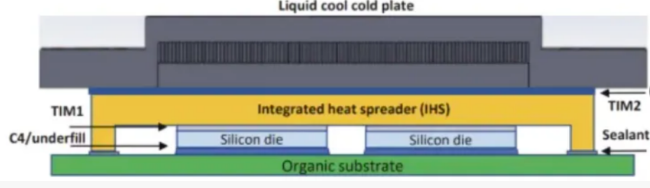
From the perspective of the chip side, the power consumption of a single NVIDIA AI chip has increased from nearly 1000W in the H200 to 1000-1500W in high-end chips based on the Rubin architecture. The core computing unit's hot spot heat flux density has exceeded 1000W/cm², far exceeding the load limit of traditional industrial cooling solutions. The theoretical thermal conductivity of traditional pure copper heat sinks is about 400W/m·K. When faced with ultra-high local heat flux density, their lateral heat spreading capacity is severely insufficient, which can easily lead to a sudden increase in temperature at the hot spot and localized thermal stress concentration in the chip. At the very least, this can result in chip frequency reduction and instability in computing power output, and at worst, it can cause packaging structure failure and a significant reduction in chip lifespan.
From the perspective of system packaging, advanced 3D stacked packaging has become the core path for enhancing computing power density. Nvidia's Rubin architecture continues and upgrades packaging technology, but it also brings about a severe "sandwich heat" issue. In the stacked structure, the heat flow transfer paths between chip layers are blocked by interposers and TSV structures, and internal heat accumulation cannot be effectively dissipated through traditional chip backside cooling solutions, becoming a core obstacle to the large-scale implementation of ultra-high-density 3D packaging.
From the perspective of the data center, traditional AI data centers account for one-third of the overall PUE in terms of cooling energy consumption. To ensure stable chip operation, the inlet water temperature of the liquid cooling system needs to be controlled within 35°C, which heavily relies on chiller cooling. This not only significantly drives up operating costs but also contradicts the green computing power requirements under the dual carbon goals. The insufficient heat dissipation capacity at the chip level directly limits the optimization space for system-level cooling solutions, forming a vicious cycle of "chip thermal management bottleneck → high energy consumption in system cooling → inability to break through in data center energy efficiency". It is precisely in this common industry dilemma that diamond materials, with their ultimate thermal physical properties, have officially entered the core stage of AI computing power from niche high-end application scenarios such as military, aerospace, and high-power lasers. The implementation of NVIDIA's Rubin architecture is a key milestone for diamond cooling technology to move from the laboratory to large-scale industrial applications.

02 Technical Decomposition of the Diamond Cooling Solution Based on the Rubin Architecture
Diamond/Copper composite heat sink
The core innovation in heat dissipation for high-end chips based on the Rubin architecture lies in the introduction of CVD diamond flakes with a thickness ranging from 100 to 300 μm into the heat sink structure, forming a composite heat sink structure with copper/tungsten metal. This represents the most technologically mature and practically feasible diamond heat dissipation solution currently available.
(1) Efficient heat dissipation of extreme hot spots: Leveraging the ultra-high thermal conductivity of diamond, it can rapidly dissipate the heat from the core extreme hot spots of the chip under ultra-high power consumption ranging from 1000W to 1500W, reducing the local heat flux density by an order of magnitude and solving the problem of sudden temperature rise at extreme hot spots.
(2) Reducing resistance and stress to enhance reliability: The thermal resistance at the interface between CVD diamond sheets and the backside of chips is significantly lower than that of traditional copper-based solutions. The gradient structure can alleviate the mismatch in thermal expansion coefficients between the chip and the heat sink, reduce cyclic thermal stress, and significantly improve the long-term operational reliability and service life of the chip.
(3) Ensuring stable computing power output: Addressing the pain point of chip overheating and frequency reduction under high load, it can ensure the continuous and stable output of computing power for Rubin architecture chips under full load conditions, avoiding computing power loss caused by thermal management constraints.
3D packaging "diamond blanket" technology
Addressing the thermal management challenges of advanced 3D packaging, NVIDIA and TSMC have collaborated to develop and validate micron-scale diamond layer growth technology (the "diamond blanket" technology) within the CoWoS 3D stacked packaging technology route, providing core technology reserves for the next generation of ultra-high-density computing power stacking. The core of this technology is to grow micron-scale ultra-thin diamond films between the chip interposers and stacked chip layers in CoWoS packaging, forming a "heat dissipation blanket" covering the heat-generating area.
Its core value is reflected in two aspects: Firstly, leveraging the ultra-high in-plane thermal conductivity of diamond films, it can quickly diffuse heat laterally between layers, evenly distribute heat accumulation within the stacked structure, and then export it through encapsulated vertical heat dissipation paths, completely solving the "sandwich heat" problem of 3D stacked chips. Secondly, relying on the excellent electrical insulation properties of diamond, when embedded between encapsulation layers, it will not interfere with chip signal transmission and electrical performance, perfectly fitting the high-density wiring requirements of advanced packaging. This technological breakthrough has completely opened up the ceiling of computing power density for 3D stacked packaging: currently, mainstream industry solutions are limited by thermal management capabilities, with the number of layers in 3D stacked chips usually not exceeding 4. However, once this technology matures, it will support the stacking of logic and memory chips with higher layers, providing core underlying support for the next generation of E-class supercomputers, as well as training and inference for trillion-parameter large models.
Chip - System Collaboration
NVIDIA's diamond cooling solution is not just an isolated chip-level technology optimization, but rather achieves full-chain collaboration from chip materials to system-level energy efficiency. Based on the significant improvement in chip cooling capability brought by diamond heat sinks, the Rubin architecture greatly enhances the cooling efficiency and thermal stability of chips through diamond cooling materials. It increases the tolerance of chips to water inlet temperature to over 45°C, allowing data centers to fully utilize natural cooling sources for refrigeration. This not only reduces the power usage efficiency of data centers to below 1.1, but also significantly reduces the equipment investment and operating costs of the refrigeration system, enabling the green and low-carbon development of AI computing power.

03 Current status of industrial application and development of diamond heat dissipation technology

The implementation of NVIDIA's Rubin architecture signifies the entry of diamond cooling technology into the large-scale application market of AI computing power. Prior to this, diamond cooling technology had undergone long-term technical accumulation, spanning from material preparation to engineering application.
In terms of material preparation, 2-4 inch large-sized CVD diamond wafers have achieved stable mass production globally, meeting the size and performance requirements of semiconductor chip heat sinks. Overseas companies such as Element Six, Coherent, and Diamond Foundry, as well as domestic enterprises like Guoji Diamond, Huanghe Whirlwind, Zhongnan Diamond, Ningbo Jingzuan, and Sifangda, have basically achieved breakthroughs in mass production, with product performance reaching the international advanced level. Previously, CVD diamond heat sinks have been applied on a large scale in high-power semiconductor lasers, phased array radar, aerospace electronic equipment, and other fields. The mature engineering experience has laid a solid foundation for their entry into the AI chip field.
In the application side, diamond heat dissipation technology has previously been constrained by cost and has only been concentrated in high-end, high-value-added fields, unable to be widely popularized in consumer-grade and industrial-grade semiconductor products. The implementation of Rubin architecture in high-end AI chips will bring large-scale market demand for this technology, driving upstream material enterprises to expand production and optimize processes, promoting rapid reduction in material costs, and forming a positive cycle of "demand growth → cost reduction → expansion of application scenarios".
In terms of technological development, the industry has formed a clear three-stage iterative route: the first stage involves the large-scale implementation of CVD diamond films for heat dissipation on the backside of high-end chips, namely the existing application solutions of the Rubin architecture and the Diamond Cooling® technology that has been commercially delivered by Akash Systems; the second stage involves the application of micron-scale diamond films for embedded heat dissipation in 2.5D/3D packaging, corresponding to the "diamond blanket" technology being developed by NVIDIA; the third stage involves the integrated application of single-crystal diamond in chip substrates and buried layers, which will fundamentally reconstruct the thermal management design logic of semiconductor chips
04 Industrial Impact and Future Analysis
Firstly, thermal management has officially become the core underlying technology that determines the upper limit of AI computing power. The implementation of diamond cooling technology has broken the physical ceiling of traditional cooling solutions, making it possible to design single-chip designs with 2000W or even higher power consumption. This will fully unleash the computing power potential of advanced manufacturing processes and 3D packaging technology, pushing AI computing power into a new stage of development.
Secondly, the energy efficiency system of data centers will undergo fundamental reconstruction. Diamond cooling technology has achieved energy efficiency collaborative optimization from the chip level to the system level, changing the traditional design logic of "cooling system adapting to chip" in data centers and shifting to a new model of "material defining cooling system". The large-scale application of warm water liquid cooling and natural cooling sources will significantly reduce the cooling energy consumption and operating costs of AI data centers, while aligning with the global trend of green and low-carbon development.
Thirdly, the superhard material industry will usher in an industrial upgrade towards high-end and large-scale development. Previously, China's diamond production accounted for over 90% of the global total. The large-scale application of AI computing power will open up a hundred-billion-yuan high-end application market for diamond materials, accelerate the domestic breakthrough in the preparation technology of large-size high-purity CVD diamond, and achieve high-quality development of the superhard material industry chain.
Fourthly, diamond materials will become a core component of the third-generation semiconductor industry. Apart from AI chips, products such as third-generation semiconductor power devices like silicon carbide and gallium nitride, high-power lasers, and radio frequency devices all face severe thermal management challenges. With the large-scale implementation of diamond heat dissipation technology in the AI chip field, costs continue to decline. In the future, it will rapidly penetrate the entire third-generation semiconductor industry, becoming the standard heat dissipation solution for high-end power devices and radio frequency devices, shaping a new industrial ecosystem.